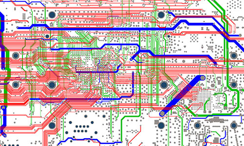
1.Net in Layout Guide Check / Impedance Check / Power Voltage Check / Power Current Check / Package Check / Net in Check 2.Placement Mechanical Check / Placement Check 3.Routing Routing Check / DRC Check / Text Check 4.Gerber Out Gerber Final Check
In order to ensure smooth inquiry process of the BOM table, please provide complete material number, packaging, and quantity. If there is a brand requirement, please specify. We can provide material preparation for both mass production and small-quantity samples.
STEP4PCB ASSEMBLE
Regardless of sample/small lot/mass production, we have diversified supply chain and material quality control with prompt delivery.